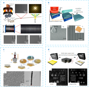
OET Inaugural Cover | 30 Years of Nanoimprint Lithography: Leading the New Era of Nanomanufacturing

Figure 1. Basic imprinting type of nanoimprinting lithography. (a) Thermal NIL developed by Chou. (b) UV-imprinting/step-flash imprinting developed by Willson.
Nanoimprinting's potential extends beyond silicon chip fabrication and wafer-scale applications. With its high throughput and 3D patterning capabilities.
CHENGDU, SICHUAN, CHINA, August 21, 2025 /EINPresswire.com/ -- Nanoimprint Lithography (NIL), first introduced in the 1990s by Professor Stephen Y. Chou at the University of Minnesota (later Princeton University), is a novel nanofabrication technology noted for its advantages in low cost, high resolution, and high throughput. The working principle involves directly imprinting mold patterns into polymeric materials, which are either cooled before demolding for thermoplastics or UV cured or thermal set for crosslinkable precursors to precisely replicate nanoscale features. With rapid advancements in science and industry, the demand for precise and efficient fabrication of semiconductor devices, optical components, and biomedical devices has significantly increased, making NIL an indispensable manufacturing method. The year 2025 marks the 30th anniversary of NIL. Through three decades of global efforts, NIL has emerged as the primary alternative to extreme ultraviolet (EUV) lithography for deep-nanoscale silicon electronics. Many semiconductor companies have recognized NIL's manufacturing quality and are actively evaluating its capability in producing advanced semiconductor devices. Moreover, with its high throughput and 3D patterning capabilities, NIL is becoming a key technology for emerging applications such as flat optics and augmented reality glasses, opening new avenues for material research and novel applications.Professor L. Jay Guo’s group from the University of Michigan published a comprehensive review titled “30 years of nanoimprint: development, momentum and prospects” in the inaugural issue of Opto-Electronic Technology, systematically summarizing key developments and future trends in NIL, with a special focus on industry advancements in nano-Si device manufacturing and nanophotonics.
The review elaborates extensively on two main NIL methods: thermal NIL (T-NIL) and UV NIL (UV-NIL), examining different types of molds, photoresists, and imprint techniques in detail (Fig. 1). For instance, plate-to-plate NIL can pattern large substrates but faces challenges in precision, high defect rates, and substantial force requirements; step-and-repeat NIL, using smaller molds repeatedly, significantly enhances precision and reduces defects; roller-based NIL offers continuous printing, greatly improving throughput but faces constraints such as curved mold fabrication, resist layer control, and demolding risks (Fig. 2). Additionally, the paper addresses core challenges in NIL, including residual layer thickness control, defect density management, and precision alignment.
Significant breakthroughs of NIL in mass manufacturing are also discussed, covering sectors like semiconductor production, flat optics, wafer-level optics, and biomedical applications. Canon's launch of the FPA-1200NZ2C, the industry's first semiconductor-grade NIL equipment, showcases high resolution, low defects, and exceptional productivity. Metalenses, a successful NIL product in flat optics, are being integrated into smartphone cameras, automotive lidar, and augmented reality (AR) glasses.
In academia, NIL research is becoming increasingly diversified and in-depth, involving high-quality optical device fabrication, precise molecular orientation control in semi-crystalline polymers, strain engineering for property tuning, and exploring emerging NIL technologies like polymer fiber imprinting, laser-assisted imprinting, ultrasonic NIL, and electrochemical imprinting (Fig. 3). These advances significantly expand NIL's applicability, paving the way for future innovations in electronics, biosensors, flexible electronics, and wearable devices.
With increasing demands for nanomanufacturing, the industrialization of NIL will inevitably accelerate. Although challenges such as defect management and alignment precision persist, ongoing process optimizations and cross-disciplinary collaborations promise to propel NIL into a new era of high-precision manufacturing.
About the Research Group:
Professor L. Jay Guo is the Emmett Leith Collegiate Professor of Electrical Engineering and Computer Science at the University of Michigan, and a Fellow of both IEEE and Optica. He has long been committed to interdisciplinary frontier research. His team focuses on the development of high-resolution lithography and nanoimprinting processes, which extend to the core areas of photonic sensors and photoacoustic sensing devices, organic and hybrid photovoltaic detectors, flexible transparent conductors, and nanostructured colors, with metasurface inverse design technology at the forefront of the international field. Leveraging cross-disciplinary expertise, the team has achieved breakthroughs in micro/nano-optical devices and semiconductor manufacturing processes The team has successfully incubated two science and technology enterprises focusing on the industrialization of flexible conductors and structural colors. With 295+ peer-reviewed publications (over 35,000 citations, H-index 93), Professor Guo serves as co-editor-in-chief of Micro and Nano Manufacturing and Editor-in-Chief of Optics and Photonics Research, and associate editor of the IEEE Journal of Photovoltaics.
Read the full article here: https://www.oejournal.org/oet/article/doi/10.29026/oet.2025.250001
Andrew Smith
Charlesworth
+ +44 7753 374162
marketing@charlesworth-group.com
Visit us on social media:
LinkedIn
YouTube
Other
Legal Disclaimer:
EIN Presswire provides this news content "as is" without warranty of any kind. We do not accept any responsibility or liability for the accuracy, content, images, videos, licenses, completeness, legality, or reliability of the information contained in this article. If you have any complaints or copyright issues related to this article, kindly contact the author above.


